Institute of
Cognitive Integrated Sensor Systems
Prof. Dr.-Ing. Andreas König

The LuCOS-Project - An HDR CMOS Image Sensor with Spiking Pixels, Pixel-Level ADC, and Linear Characteristics
Subject:
Implementation of a novel sensor concept in a
state-of-the-art technology for demonstration and evaluation of sensor samples
and their application in image processing and pattern recognition
applications.
Abstract:
In the research project with an industrial partner in a consortium of two
partners, the objective was to develop an image sensor for machine vision
purposes with high intrascene dynamic range, broad spectral sensitivity, linear
characteristics, pixel-level ADC with variable resolution, and minimum FPN
implemented in a standard CMOS technology for cost-sensitive embedded vision
systems and applications. The system
architecture, including an inteligent camera, was designed and implemented by
the industrial partner Sarad GmbH, the sensor
design and chip implementation was devised as the university contributors.
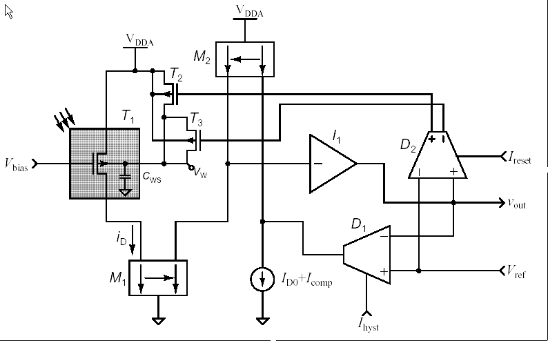
The investigated pixel structure, which was elaborated in prior work by Streil and Klinke, uses the well-substrate junction within a CMOS-inverter as photo-sensitive element. Light induced charge accumulation is thresholded by following sensor electronics and the junction capacitance is cyclically drained by a transistor switch. A spike is generated for each reset by the switch transistor. Thus, a spike train with illumination dependent frequency is generated. A simplified schematic of the analog part of the pixel cell is given below. Details can be taken from the corresponding publication.
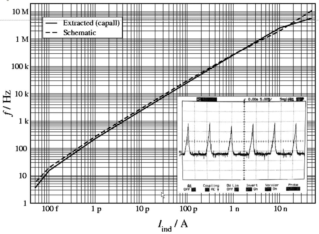
For the chip design Austriamicrosystems 0.8mm technology was employed. The figure below gives the simulation result of the spiking frequency vs. the simulated photo current, which shows a linear relationship for more than five decades. Further, a sample spike train is given.
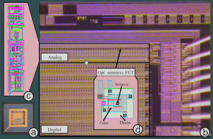
Pixel-level ADC takes place by counting of the spikes of the resulting spike trains. For this aim, asynchronous counters with 12 and 20 bit, respectively, have been implemented in two successive row sensor chip design efforts. These chips were denoted as LuCOS chips, LuCOS1k128 and LuCOS1M128, respectively. The analog pixel cell, indicated by c) in the figure below, employs 26 transistors and has a length of 154 mm with a pixel pitch of 25 mm. Particular attention has been paid to the judicious layout design of the photo sensitive FET d) to reduce parasitic effects and improve pixel reproducibility. The counter stages consumes 113 mm per bit at the same pixel pitch. The LuCOS1k128 a) features 63,260 transistors, 128 pixels with 12 bit counters stages and a die size of 4.12x2.21 mm2.
In the LuCOS architecture, resolution can be traded-off for speed by using only a fraction of the counter range at higher readout speed. Thus, the approach is promising both for high-speed as well as high dynamic range applications.
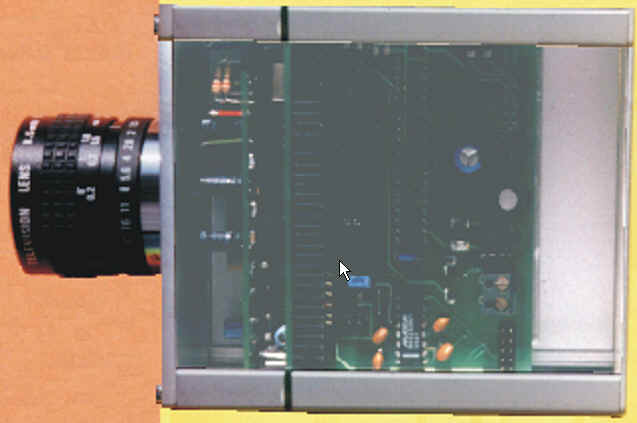
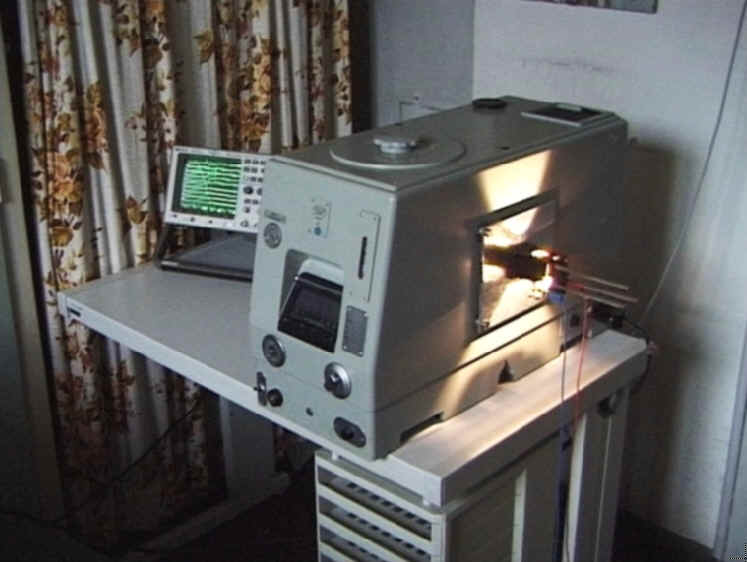
The LuCOS1k128 could be successfully tested. By Sarad GmbH a modular intelligent camera, given below on the left, was designed implemented to support in-situ test of the LuCOS chips and to serve as a platform for following practical implementation. The camera system boards also served for sensor characterization based on the monochromomator setup given below on the right.
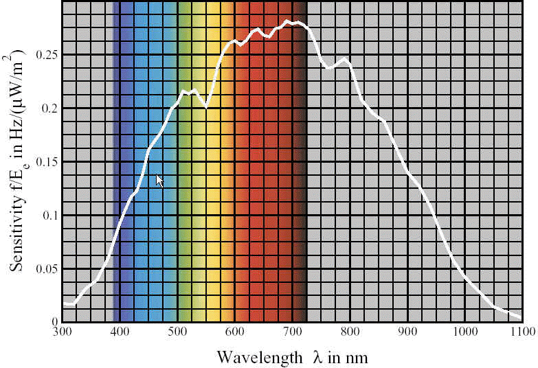
The resulting spectral sensitivity determined for LuCOS1k128 is given below. The broad spectral sensitivity is well suited for the machine vision applications this design activity targets on.
The objective of the project, to show the feasibility of this particular image sensor architecture, has been reached. The simulation and measurement results of the LuCOS1k128 and in part of the LuCOS1M128 show that numerous extensions are required to fully exploit the concept. A redesign in a leading edge technology is mandatory, both for reasons of increased speed, and thus dynamice range, as well as size issues with regard.to viable row sensor sizes for industrial applications, e.g. 2048 pixels and three rows. Further, extension of the concept to color image registration is another potential line of development.
| Status: | concluded, duration 10/1999-03/2000 | ||
| Partner: | SARAD GmbH, Wiesbadender Strasse 20, 01159 Dresden (Prime contractor) | ||
| Financing: | Freestate of Saxony and the European Union (via
the Sächsische Aufbaubank SAB; prime contract: Grundlagen
der Optosensorik auf der Basis von intelligenten CMOS P-Kanal
Transistorstrukturen, sub contract: VLSI-Entwurf
eines prototypischen innovativen Optosensors für einen Kamerademonstrator) |
||
| Contact: | Prof. Dr.-Ing. Andreas König | ||
Contributors: |
Jens Döge, Andreas König (Subcontractor TU Dresden), Gerd Schönfelder, Thomas Streil (Prime contractor, SARAD GmbH) | ||
| Publications: | |||
| J. Döge, G. Schönfelder, T. Streil, and A. König. An HDR CMOS Image Sensor with Spiking Pixels, Pixel-Level ADC, and Linear Characteristics. Brief paper IEEE Transactions on Circuits and Systems TCAS II, pp. 155-158, February, 2002. | |||