Institute of
Cognitive Integrated Sensor Systems
Prof. Dr.-Ing. Andreas König

Instant Design Validation & Measurement Experience
![]()
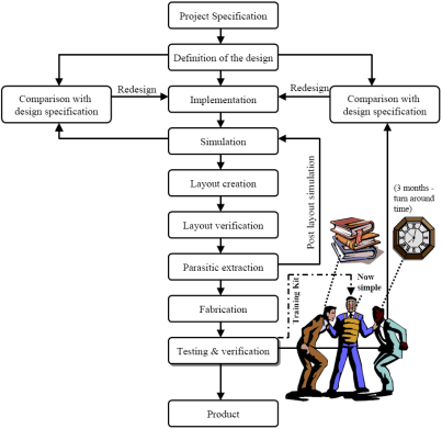
The TESYS analog and mixed-signal integrated circuit design course will take students through the whole design cycle and acquaint them with the tasks in each step using the design of an application specific operational amplifier as a common example.
The following table gives a typical specification handed-out to students as part of the task description for the semester project:
S.Nr |
OpAmp characteristics |
Specification Request |
1 |
Open loop gain |
>70 dB |
2 |
Gain band width |
1 MHz |
3 |
Phase margin |
>60° |
4 |
CMRR |
>80 dB |
5 |
Common mode range |
-0.8 V to +0.8 V |
6 |
Output range |
-0.35 V to +0.35 V |
7 |
Voltage supply |
-1.65 V to +1.65 V |
8 |
Slew rate |
1 V/µsec |
9 |
Settling time |
1 µsec |
10 |
Load capacitance CL |
5 pF |
11 |
Load resistance RL |
100KW |
12 |
Power dissipation |
Minimum, < 1mW |
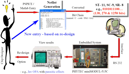
A bias of this specification to Miller-topology is obvious and motivated by the fact, that the currently available reconfigurable chip is limited to Miller and Folded-Cascode amplifiers. According to the above specification table, students start sizing the amplifier devices to meet the specifications. This can be achieved by manual design, e.g., following the design plans from Allen/Holberg, by table-based calculation employing Excel or Matlab, or circuit sizing by Genetic Algorithms or Particle-Swarm-Optimization. The sizing values confirmed by circuit simulations in Cadence DFW II have to be quantized to the resolutions of the scalable active and passive devices of the FPMA.
S. Nr |
Device Name for Fig. 6 |
Device Sequence in FPMA |
Device Dimensions from Matlab (L=1µm) |
Corresponding Bit Patterns |
OpAmp Characteristics |
Obtained Results |
1 |
M1 |
C1 |
4 pF |
100100000 |
Open loop gain |
72 dB |
2 |
M2 |
M6 |
W = 154µ |
10010111111 |
Gain band width |
5 MHz |
3 |
M3 |
M7 |
W = 2µ |
00000010000 |
Phase margin |
60 ° |
4 |
M4 |
M2 |
W = 66µ |
01000010000 |
CMRR |
86.7 dB |
5 |
M5 |
M1 |
W = 66µ |
01000010000 |
CMR |
- 1.4 V to + 1.4 V |
6 |
M6 |
M5 |
W = 154µ |
10010111111 |
Output range |
- 1.3 V to + 1.3 V |
7 |
M7 |
M4 |
W = 1µ |
00000001000 |
Slew rate |
2 V/ µsec |
8 |
C1 |
M3 |
W = 1µ |
00000001000 |
Settling time |
1.2 µsec |
9 |
--- |
--- |
--- |
--- |
Power diss. |
0.3 mW |
The follwoing sketch explains the representation of each amplifier transistor by a scalable devices, which is actually a reconfigurable field, which defines the width of a transistor from the configuration bitstring. The sizing information of all amplifier devices is concatenated and clocked into the FPMA chip given below.
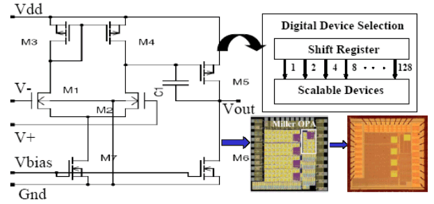
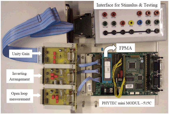
The FPMA-1 chip is integrated in a simple miniModul-515C embedded system of Phytec. The bitstring is written by the dedicated software interface of that system to the FPMA-1 and at the end of the programming cycle enables the reconfigurable amplifier for measurement. The amplifier can be put into typical feedback conditions by tiny plug-in boards, e.g. inverting or unity gain arrangements can be achieved easily for measurement purposes.
The following figure elucidates the overall reconfiguration and measurement cycle, including the option of design improvement by configuration modification.
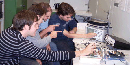
The 2007 students group active in measuring the properties of their respective amplifier sizings embodied on the FPMA-1 platform.
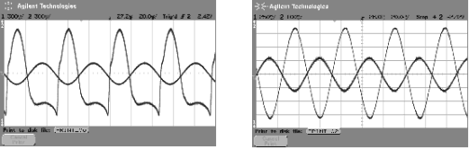
An unfortunate configuration (left) and an acceptable configuration (right) and corresponding results of an inverting operational amplifier are shown in the next two figures grabbed from the MSO visible in the background above.
Finally, the oral examination based on semester project takes place. This involves a twenty minutes presentation followed by interrogation on the project, the design decisions, encountered problems, and achieved results.
In future extensions, the design of a more complex and versatile FPMA-chip and its exploitation for designers' training is aspired.