Institute of
Cognitive Integrated Sensor Systems
Prof. Dr.-Ing. Andreas König

Advanced Methods for the Analysis of Semiconductor Manufacturing Process Data
Subject:
The analysis, control, and optimization of manufacturing processes in semiconductor industry is an application with significant economic impact. Modern semiconductor manufacturing processes feature an increasing number of processing steps with an ever increasing complexity of the steps themselves and generate a flood of multivariate monitoring data. This exponentially increasing complexity and the associated information processing and productivity demand imposes stringent requirements, which are hard to meet by state-of-the-art monitoring and analysis methods and tools. The work deals with the application of selected methods from soft-computing, also applied in the optimized and automated design of intelligent multi sensor systems, to the analysis of deviations from allowed parameters or operation ranges, i.e., anomaly or novelty detection, and the discovery of nonobvious multivariate dependencies of the involved parameters and the structure in the data for improved process control. Methods for on-line observation and off-line interactive analysis employing novelty classification, dimensionality reduction and interactive data visualization techniques are investigated in this feasibility study, based on an actual application problem and data extracted from a CMOS submicron process. The viability and feasibility of the investigated methods are demonstrated with real process data.
Abstract:
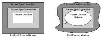
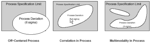
The ongoing growth in semiconductor industries, predicted and driven by Moore's law, leads to a rapid complexity increase in semiconductor manufacturing processes. The number of manufacturing stations, required processing steps, and related parameters rapidly increase and mandatory process monitoring returns a flood of multi-variate data. Yield requirements demand for tight process control. The monitoring such a complex process, which can be met in similar instances in general in industrial manufacturing, however, requires on-line monitoring and decision making as well as ensuing extraction of nonobvious information and structure in the data. Such a procedure of knowledge discovery and the mentioned on-line decision making serve to control the respective complex process, e.g., for quality assurance purposes, keeping the process in a multivariate window of allowed parameter tolerances. Typical aims in semiconcductor manufacturing are the centering of the process in a so-called process window and the assurance of an optimum yield based on functional and electrical tests. The following figure illustrates the concept of a process window:
From the proprietary software system and company database affiliated to
the regarded manufacturing process, a subset of data generated for the processing
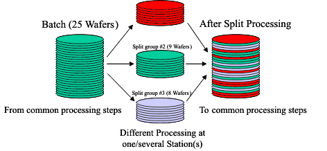
two wafer lots with five measurement positions for each wafer was
extracted as experimental data. A split of three, i.e., a partitioning of each wafer batch into three
subgroups for individual processing of each partition was carried out during
production. The data was converted by Ecxel to our proprietary QuickCog system. A database of 220 vectors
with 205 dimensions is the baseline in the following experiments. It will
be denoted by SPLIT in the following. The size of this database is given by
the typical wafer batch size of 25 times the five measurement sites per wafer. Complementing the parameter data, class affiliations were generated in
two files. A three classes file was generated, regarding split information only
for the complete database. The data labeled by this class file will be denoted
by SPLIT3 in the following. Additionally, a six classes file was generated according
to lot and split affiliation of each wafer/measurement location. The
labeled data will be denoted by SPLIT6 in the following. Additionally, according
to the underlying lots the data have been separated in two databases
denoted by SPLITTrain3 and SPLITTest3 with three classes each, corresponding
to the underlying split of 3 of each lot. Finally, for the novelty
classification purposes, a training set was extracted from the first lot and
containing data only from one split. This will be denoted by SPLITTrain-
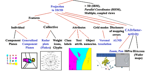
OCC in the following. The following figure show a taxonomy of visualization techniques, with those techniques emphasized, that have been employed to the semiconductor data:
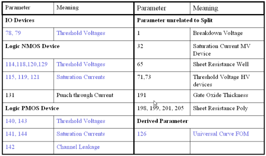
Various selection methods and experiments were conducted and the results of the AFS application were investigated with regard to their meaning, and thus, usefulness for pratical application. The following table shows, that the key variables with regard to the split were discovered:
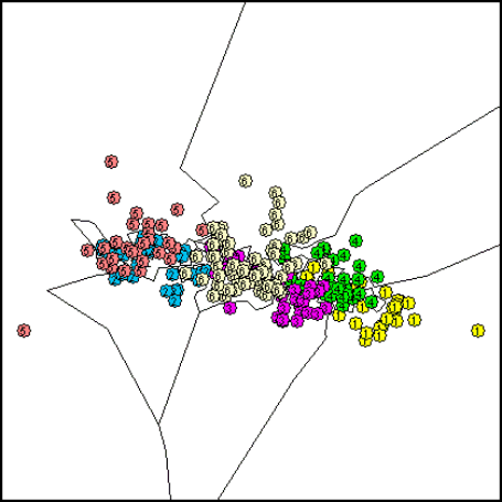
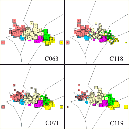
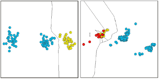
In future work, more advanced feature selection techniques, employing evolutionary techniques, can be considered for this problem, e.g., to deal with larger and different data sets. In the next step of supervised analysis, classification was applied to the data base after AFS downto 9 significant variables. A basic nearest neighbor technique (Reduced-Nearest-Neighbor, RNN) was employed with the first lot for training and the second for testing. The number of classes goes down from L=6 to L=3, as only the split groups are regarded. The lot affiliation is discarded and actually represented by train or test set affiliation. The results are illustrated in the following figure:
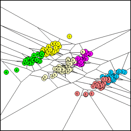
Obviously, classification accuracy of 100% was achieved in generalization. Thus, no other classification techniques, such as RBF, PNN, or SVM, have been regarded here. However, as anomaly or novelty detection is a very important concept in (on-line) process monitoring and deviation detection, related concepts of one-class-classification (OCC) were studied next. A NOVCLASS classifier was developed and applied, that uses hypersphere classifier concepts, similar to the famous RCE model, however, the stored hypersphere centers relate only to known, normal data and the radii are computed from observed deviations in the normal or non-novel data. Thus, as sketched in the following figure for the two-dimensional case, a non-parametric mapping of normal regions in feature space is achieved:
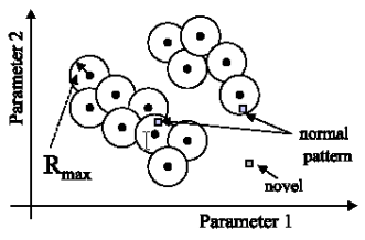
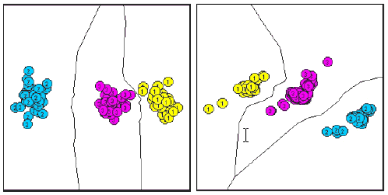
In the classification step, anomal or novel patterns are detected, if they drop in outside of the union of all normal hypersheres. Training in the particular case was carried out based only on 30 references from class 1 of the first lot. In resubstitution, all novel measurements were correctly classified by OCC. In generalization, only 87.2 % were achieved, which is illustrated in the following figures:
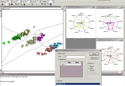
The errors occured for normal data, that was classified as anomal or novel. Obviously, the little training data made OCC too sensitive with regard to existing variations in the normal data itself. More extensive training data as well as more sophisticated Rmax computation can be considered as effective remedies. The concept of OCC and novelty detection is applicable also other domain, e.g., visual inspection in industrial manufacturing (see also the ISE NOVAS algorithm). From the investigations, feasibility and saliency of the regarded methods for this application domain could be shown. The need for method and in particular tool improvement and domain-specific specialization was detected. A first version of an improved interactive visualization & analysis tool, derived from the Acoustic Navigator, was established and tried (The support of Michael Eberhardt for this part of the work is gratefully acknowledged here). The following figure shows the view of the new Semiconductor-Navigator tool at work:
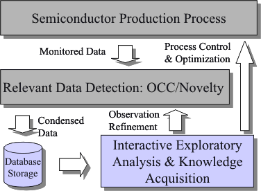
Finally, the first sketch of a system architecture for semiconductor manufacturing data analysis and process control for yield optimization has been suggested:
The presented work contributes to the industrial application of advanced softcomputing
methods in the field of semiconductor manufacturing process data
analysis. In particular, fast and efficient methods for multivariate data dimensionality
reduction including automatic methods for parameter (AFS) or parameter
group saliency detection, and interactive visualization have been investigated
in this first feasibility study. On-line visualization of the process trajectory in
the multivariate space is also feasible by available fast methods for adding
new data vectors in an existing mapping. The application of more recent methods, e.g., PSO-based and/or multiobjective AFS, and an integrated working environment will be required and highly beneficial for the regarded task. In particular, OCC or novelty detection is a promising concept for this and other applications. More information can be found in the reference given below.
| Status: | concluded, elaborated in 2001/02 | ||
| Partner: | Infineon OhG, Dresden | ||
| Financing: | Infineon OhG, Dresden | ||
| Contact: | Prof. Dr.-Ing. Andreas König | ||
| Contributors: | Andreas König and Achim Gratz | ||
| Publications: | |||
| A. König and A. Gratz. Advanced Methods for the Analysis of Semiconductor Manufacturing Process Data. Book chapter in Advanced Techniques in Knowledge Discovery and Data Mining, N. R. Pal, L. C. Jain (eds.), Springer, pp. 27-74, ISBN: 1-85233-867-9, February, 2005. | |||
| König, Andreas: "How Could Semiconductor Industry Benefit from the Evolution of Soft-Computing Methods ? Suggestions for Dimensionality Reduction and Interactive Data Visualization" Handout of Invited Talk, SEMATECH Yield Council Meeting, Forum Hotel, München, Germany, May 7th, 2003. |